Difference between revisions of "PG31 GPS RS232 Dev Board"
(Remove spam links, you should clean this or block any changes.) |
m (Protected "PG31 GPS RS232 Dev Board": spam magnet [edit=autoconfirmed:move=autoconfirmed] (expires 05:27, 2 March 2008 (UTC))) |
||
| (3 intermediate revisions by 3 users not shown) | |||
| Line 1: | Line 1: | ||
| + | {| align=right | ||
| + | |- | ||
| + | | | ||
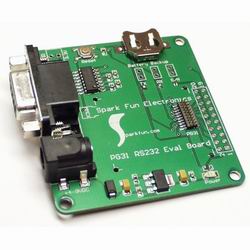
[[Image:Main-Eval-PG31-RS232.jpg|PG31 RS232 Dev Board]] | [[Image:Main-Eval-PG31-RS232.jpg|PG31 RS232 Dev Board]] | ||
| − | + | |} | |
<b>Description:</b><br> Getting information from your project to your computer can be difficult at first. Once you discover how to setup an RS232 connection, it's really just cut-and-paste for future projects. | <b>Description:</b><br> Getting information from your project to your computer can be difficult at first. Once you discover how to setup an RS232 connection, it's really just cut-and-paste for future projects. | ||
Latest revision as of 22:27, 30 December 2007
Description:
Getting information from your project to your computer can be difficult at first. Once you discover how to setup an RS232 connection, it's really just cut-and-paste for future projects.
In this project we demonstrate how to:
- Setup an external power supply
- Setup 3.3V to RS232 circuit
- Complex PG31 GPS footprint
Contents
Power Regulation
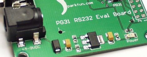
First we will start with a simple adjustable voltage regulation circuit:
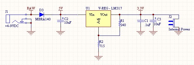
Please note this is a relatively compact SMD version of the power supply. This can easily be obtained with through-hole components using a breadboard. Here is the schematic:
Now let's discuss what's going on here. The barrel jack (J1) is a basic 5.5mm OD 2.1mm ID type jack. We get an unregulated 9-13V out of the wall wart.
The D3 large diode MBRA140 is for reverse protection. It can handle up to 1A and prevents damage to the board if a center-negative wallwart is attached. This diode will cause a ~0.5V drop from whatever the wall-wart is outputting.
C2 (10uF Tantalum Capacitor in this case) is a basic decoupling cap. 10-100uF is adequate but should be rated for 15-25V.
U1 is the LM317 (or LM1117 in SMD form) adjustable voltage regulator. It will take in some larger voltage and output a set voltage. The output voltage is set with two external resistors. R1 is historically 240 and value for R2 is different for different required output voltages. In our case, we want 3.3V out of the regulator, so R2 is set to 715. The LM317 is good because it is variable, the SOT-223 package is nice becuase it can take a relatively large voltage on the input (25V max I believe?) and has decent heat dissapation.
C1 and C3 are decoupling caps that help clean up the output transcients and noise.
J2 is just a two pin polarized header so that you can either 'steal' 3.3V from the board to power other boards, or have other boards power this board without the need for the external wall wart.
RS232 Interface
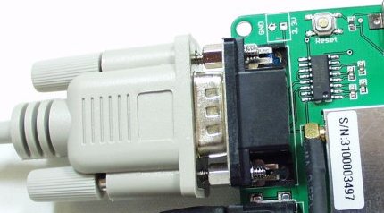
So we've got a nice clean output of 3.3V from the regulator, let's look at the RS232 connection:
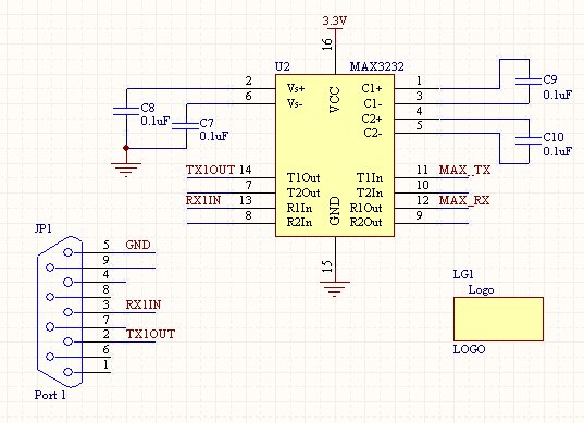
This shows the DB9 connector (also known as a D-Sub 9-pin connector), serial cable, and MAX3232 IC and charge pump caps (all SMD, again, can be done with PTH components). Here is the schematic:
Now read-up on the MAX232 IC. It could be the most common IC out there, at least for the embdded world. This IC will have many different model names (ICL232 for example) but all do the same thing, and will most likely have identical pin-outs. This IC is used to take low voltage signals from your micro or PIC or ARM or whatever, and converts those low-voltage signals to higher-voltage signals that the computer can understand. The voltage levels on TTL are also inverted for RS232 so the MAX232 takes care of that as well!
The MAX232 takes in TTL signals and sends out RS232 signals. It also takes the RS232 signals from the computer and outputs TTL signals to whatever microcontroller you are using. How does it do this magic? With charge pump capacitors. You'll notice four 0.1uF caps attached to the MAX3232. If you're reading closely, you'll also notice we have a MAX3232 not the MAX232. Difference:
- MAX232 must be powered with 5V and converts 5V TTL<->RS232
- MAX3232 can be powered from 3V to 5V and converts it to RS232
So in this application, the GPS unit is running at 3.3V. If we were to send 5V TTL to it, it would be damaged! So we must use the lower voltage MAX3232 part. No big deal, it's functionally identical to the MAX232. From here on out, I will only refer to the MAX232.
When you first view the MAX232 component, it can be a bit confusing. The pins label T1/T2 are the transmit channels (MAX232 has 2 TX channels and 2 RX channels). T1In/T2In will take *in* TTL and send *out* RS232 out T1Out/T2Out. So for our purposes, we need to connect the GPS unit's serial TX pin to the T1In pin of the MAX232. So when the GPS unit outputs some 3.3V TTL signals, these signals will be converted into RS232 and sent to the computer (TX1Out is connected to pin 2 on the DB9 connector).
Finally, when the computer needs to send info to the GPS unit, it will send RS232 signals down the serial cable, on pin 3 of the serial cable/DB9 connector to R1In of the MAX232. This RS232 signal will be converter to TTL and sent out the R1Out pin. This TTL signal is connected to the RX pin on the GPS unit. Voila.
I can't tell you how many times I've crossed TX and RX on different projects. Sit down, think about it, and once you've got it wired correctly, cut and paste into future projects.
PG31 Footprint
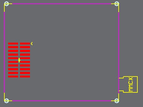
Now about the footprint for the PG31. Unless the manufacturer hands you a foorprint file or a simple, recommended FP in the datasheet, you're going to have to go it on your own. We took the PG31 and a pair of calipers and went at it. It can be extremely difficult the first time. This PG31 FP took me twice to get correct. Do the best you can and try to account for things like the antenna connector. The second rev FP, I forgot to account for the MMCX connector, I put the DB9 connector right up against the PG31, and Viola - useless PCB! a.k.a another coaster for my coffee cup. But once you've got the FP, you're good for all future projects using that device. Now you know why engineers hate to change parts...
Final Layout
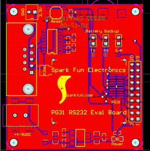
You can see the PCB layout is pretty straight forward. The 'solder jumpers' are a feature that SFE came up with to minimize our manufacturing time while allowing end users to populate the physical jumpers if they needed the ability to connect/disconnect a feature often and quickly. Most users just plug the PG31 onto their computer for quick evaluation. At some point, the MAX232 may need to be disconnected from the circuit so that an external micro or embedded system could be attached. If this is done back and forth often, the end user can clear the solder jumper with a swipe of the soldering iron, install a 2-pin header and a black plastic jumper. This now allows them to jumper/dejumper quickly and keeps us from having to solder the 2-pin headers into a board that may not need them.
Things to Improve
So that's pretty much it. The board works well, and assuming Laipac doesn't change their parts again, we will produce the board for some time.
Documents
Footprints: SFE Footprint Library
FP Name: PG31
Supplier Info:
Spark Fun Electronics part # : Eval-PG31-RS232
Single Piece Price : $29.95
Related Items:
